The AI Compute Supply Chain
Mapping Every Bottleneck From Sand to Inference
A field guide for the technically literate but market-curious: first what actually goes into building and running an AI model, then the entire physical chain behind it — who benefits financially at each stage, and where it is genuinely bottlenecked in 2026.
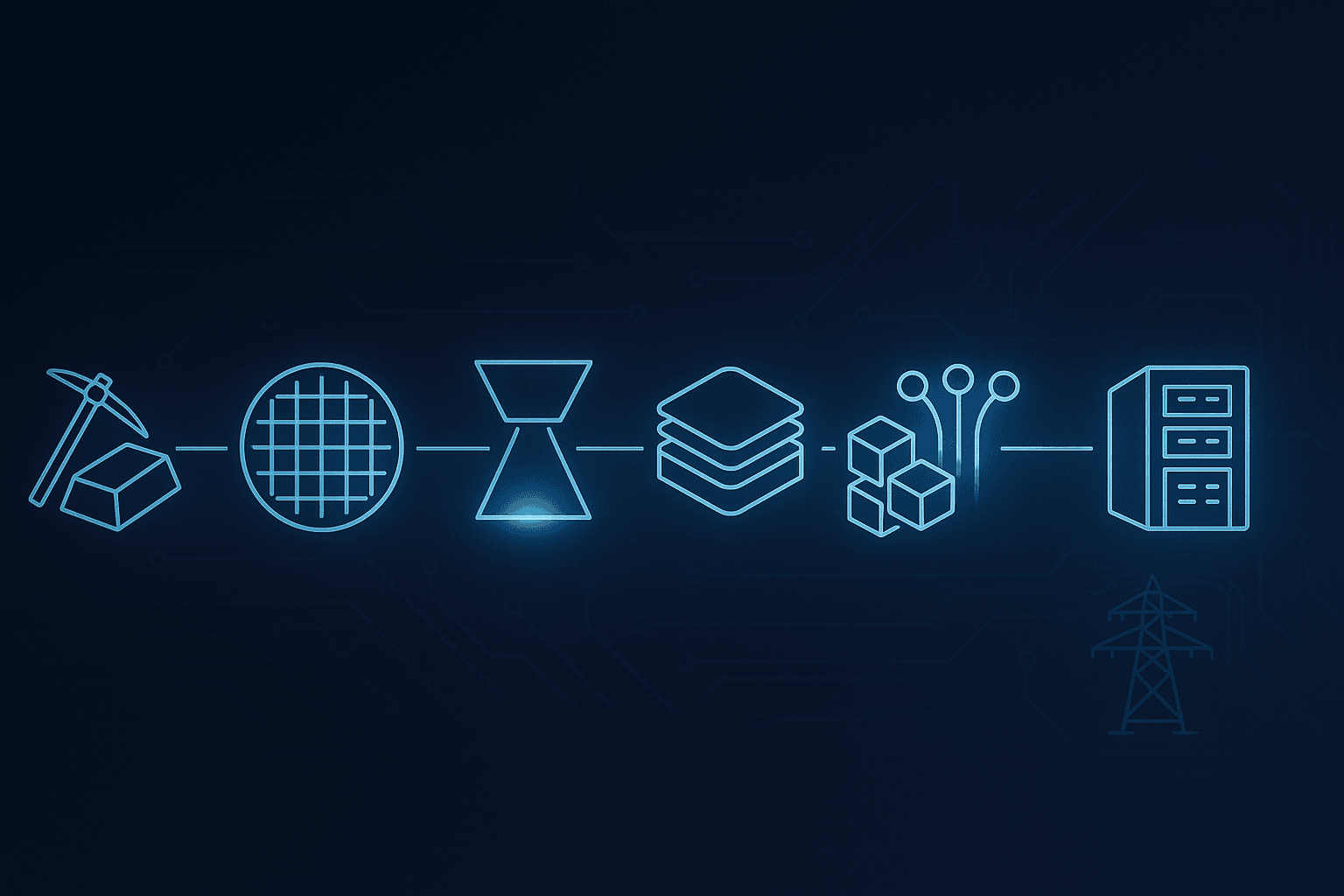
The core thesis
For a decade, "more AI" meant one thing: more compute. That era is over. AI's binding constraint has migrated from raw chips into a systems problem that spans copper mines, a single lithography vendor, advanced chip packaging, high-bandwidth memory, optical interconnect, and — increasingly — the electrical grid itself. You cannot reason about which parts of this chain are scarce, who profits, and what is over-hyped until you understand what training and inference actually demand from hardware. So we start there, then walk the chain stage by stage, marking each one's bottleneck and asking the only question that matters for an investor: is this already priced in, does it still have room to grow, or is it genuinely contested?
Underpriced
Advanced packaging, grid power, NAND storage
Contested
Custom silicon vs Nvidia, neoclouds, photonics timing
Largely priced in
Nvidia, ASML, the copper macro story
Contents
It's a long read — jump to what you need. Every stage is self-contained: bottleneck, who's exposed, verdict.
Part 1 — The primer
Wrap-up
The Primer — what actually happens when you build and run an AI model
Before any supply chain talk, you need a working mental model of where the hardware goes and why. Every component downstream exists to serve one of the steps below.
What a model actually is
An AI model is, at bottom, a very large pile of numbers. During training the model adjusts those numbers until it gets good at predicting the next word (or pixel, or token). Once training stops, that frozen pile of numbers is the model. Everything else — the chips, the memory, the data centers — exists to either produce that pile or to run it.
Parameters / weights
The individual numbers inside a model that were learned from data. A model with 'one trillion parameters' is literally storing and doing math on a trillion of these numbers. More parameters generally means more capability — but also more compute to train and more memory to hold.
Analogy: Picture an enormous recipe with billions of precise measurements — a pinch more here, a little less there. Training is tasting the dish over and over and tweaking every measurement until it comes out right. A model with more parameters is a recipe with more ingredients to balance — and it needs a far bigger kitchen just to lay them all out.
This is the first link to the supply chain: a trillion parameters do not fit on one chip. They have to be split across many chips, which forces those chips to constantly talk to each other. Hold that thought — it is the reason interconnect and memory bandwidth end up mattering as much as raw compute.
The transformer — and why we must be careful with that word
Transformer (AI architecture)
The neural-network design introduced in 2017 that lets a model weigh how every word in an input relates to every other word, all at once, in parallel. That 'all at once' is the key property — older architectures processed text one step at a time, which was slow and lost long-range context.
Analogy: An older model reads a sentence like a person with a finger under each word, one at a time. A transformer (AI) lays the whole page on a table and looks at how every word connects to every other word simultaneously. That parallel 'look at everything at once' is exactly the math GPUs are built for.
Training vs inference — two workloads, two very different hardware demands
This distinction is the single most important idea in the whole piece, because it determines what hardware is scarce and why.
Training vs inference
Training is the one-time (or periodic) job of teaching the model: a massive computation run across thousands of chips for weeks or months to set all the parameters. Inference is running the finished model to answer a request — and it happens constantly, in parallel, for every user prompt, forever.
Analogy: Training is the model doing months of homework to learn the subject. Inference is the model sitting the exam — over and over, a fresh exam for every single user request, every second of every day. Homework is a huge one-off cost. The exams never stop, so speed and cost per exam are what dominate the economics.
Training — pay once, enormous
- •One giant synchronized job across 10,000–100,000+ chips
- •Runs for weeks to months
- •Bottleneck: getting tens of thousands of chips to act as one computer — interconnect is king
- •A capital project: build it, run it, get a model out the other side
Inference — pay forever, relentless
- •Millions of small independent requests, in parallel, 24/7
- •Latency and cost-per-query dominate everything
- •Bottleneck: memory bandwidth — feeding the model's weights to the chip fast enough
- •An operating cost that scales with every user you add
Why transformers favor GPUs over CPUs
GPU vs CPU
A CPU (central processing unit) has a few very powerful cores that do complicated tasks quickly, one after another. A GPU (graphics processing unit) has thousands of simpler cores that all do basic math at the same time. Transformers are mostly one operation — multiplying big grids of numbers (matrix multiplication) — repeated billions of times, which is exactly the 'lots of simple math in parallel' that GPUs win at.
Analogy: A CPU is a few PhDs solving hard problems sequentially. A GPU is ten thousand bright high-schoolers all doing arithmetic at once. For one tricky logic puzzle you want the PhDs. For multiplying a million pairs of numbers right now, the crowd of high-schoolers obliterates them.
Because a transformer (AI) is built on enormous parallel matrix multiplication, the GPU's thousands-of-cores design is a near-perfect fit and the CPU is hopelessly outmatched. This is why the AI boom is a GPU boom — and why an entire supply chain has reorganized itself around feeding GPUs.
The memory and bandwidth crisis bigger models created
Here is the chain reaction that explains half of this article. Models got bigger. A model with a trillion-plus parameters does not fit in the fast memory attached to a single GPU. So you split it across many GPUs. But split parts of one model must constantly exchange intermediate results — so the chips have to talk, fast and continuously. Two things therefore became as important as the GPU's raw math: how much fast memory sits next to each chip, and how quickly chips can move data to memory and to each other.
DRAM and HBM (first pass)
DRAM is fast, temporary working memory — where a chip keeps the data it is actively using. HBM (high-bandwidth memory) is DRAM that has been stacked into vertical towers and bolted right next to the GPU so data can flow between them extremely fast. HBM is not a different material from DRAM; it is DRAM in a much higher-performance package.
Analogy: DRAM is the open notebook on your desk — quick to read and write, wiped when you finish. HBM is that same notebook, but thickened into a stack and clamped against the processor so it can flip pages many times faster. (We will meet NAND — the filing cabinet — later.)
The software stack — and Nvidia's real moat
Hardware is only half the story. There is a software stack between a researcher's code and the silicon, and it has three layers worth naming in plain terms:
Framework
e.g. PyTorch
Where humans describe the model — the architecture and the math, in readable code.
Compiler / driver layer
e.g. Nvidia CUDA
Translates that math into instructions the specific chip can run efficiently, and squeezes out performance. This is the layer that took 20 years to mature.
The chip
the GPU / accelerator itself
Executes the instructions. Fast silicon is necessary but, on its own, not sufficient.
Anatomy of an AI data center
Put it together and a modern AI data center is a surprisingly physical object. Racks of GPUs are wired together with ultra-fast interconnect into one giant computer. Each GPU is fed by HBM sitting millimeters away and by NAND storage holding the datasets. The whole thing runs so hot that air cannot cool it, so liquid is piped directly to the chips. All of it is drawn from the electrical grid through (electrical) transformers and switchgear, and orchestrated by software schedulers that decide which job runs where. Remove any one of these — chips, memory, interconnect, cooling, or power — and the data center does not run. That is the supply chain we are about to walk.
The Supply Chain — from raw materials to inference
For every stage we answer three things: (a) what the bottleneck is and why it physically or economically exists, (b) which public companies benefit and how directly, and (c) a verdict — priced in, room to grow, or contested.
The chain is only as fast as its slowest stage. In 2026 the binding constraints are not raw compute — they are advanced packaging (CoWoS), high-bandwidth memory, and grid power.
Raw materials: copper and critical minerals
The chain begins underground. Before a single chip exists, an AI data center needs staggering quantities of copper — and copper is dug out of the ground on geological timescales, not AI timescales.
Copper is the metal of electrification. It carries power from the grid into the building, distributes it through busbars to every rack, and increasingly forms the tubing and cold plates of liquid cooling. A single large AI data center can require on the order of 50,000 tonnes of copper. And AI is not replacing existing copper demand — it is stacked on top of an already-tight market being pulled by EVs, renewables, and grid modernization.
| Company | How it is exposed | Verdict |
|---|---|---|
| Freeport-McMoRanNYSE: FCX | Largest publicly traded copper producer; the most direct large-cap copper proxy. Earnings highly geared to the copper price. | Contested |
| Southern CopperNYSE: SCCO | Vast reserves and low costs; pure-play exposure but premium valuation and Latin American jurisdiction risk. | Contested |
| BHP / Rio TintoNYSE: BHP / RIO | Diversified majors with growing copper books; AI-copper is a small slice of a much larger iron-ore-driven business. | Priced in |
| Copper miner ETFse.g. COPX | Basket exposure to the theme without single-mine risk; the simplest way to own the macro story. | Room to grow |
Chipmaking equipment: lithography and the 'picks and shovels' layer
To make a chip you first need the machines that print chips. This stage sits upstream of even TSMC — and it contains the single most extreme chokepoint in the entire chain.
Wafer
A thin, polished disc of ultra-pure silicon, usually 300mm across. Chips are not made one at a time; hundreds are fabricated together across the surface of one wafer, then cut apart at the end.
Analogy: A wafer is a sheet of cookies. You print the whole sheet at once, then cut individual cookies (chips) out of it. A defect anywhere on the sheet ruins the cookies it touches.
EUV lithography
Lithography is printing the circuit pattern onto the wafer with light. The smaller the features you want, the shorter the wavelength of light you need. EUV (extreme ultraviolet) uses light so short that only one company on Earth has ever built a working production machine for it — and the most advanced chips simply cannot be made without it.
Analogy: Lithography is a stencil-and-spray-paint step for circuits. Ordinary light is a fat spray nozzle; you can only paint chunky shapes. EUV is an impossibly fine airbrush that can paint lines a few atoms wide. Below a certain chip size, the fat nozzle physically cannot draw the picture — you must have the airbrush.
| Company | How it is exposed | Verdict |
|---|---|---|
| ASMLNASDAQ: ASML | Absolute monopoly on EUV; every leading-edge AI chip in the world is printed on its machines. Record bookings and a large multi-year backlog tied directly to AI capex. | Priced in |
| Carl Zeiss / Zeiss SMTprivate (within Zeiss) | Sole supplier of the ultra-precise EUV optics ASML depends on. Not directly investable as a pure play, but the deepest sub-supplier moat in the chain. | Room to grow |
| Applied Materials, Lam, KLAAMAT / LRCX / KLAC | The rest of the fab toolset — deposition, etch, metrology. Benefit from every new fab regardless of who wins at the leading edge. | Room to grow |
Wafer fabrication and advanced packaging
The most underappreciated bottleneck in the entire chain in 2026 is not making the chip — it is gluing the finished chip and its memory together. This step, called CoWoS, is the binding constraint.
Fabrication is where the wafer becomes working chips. Each individual chip on the wafer is called a die. Because no process is perfect, some dies come out defective; the percentage that work is the yield, and yield is what separates a profitable node from a money pit. TSMC's leading-edge nodes (N3, and soon N2) are effectively sold out. But raw wafer supply is not the tightest link. The tightest link is what happens after the wafer is cut.
CoWoS / advanced packaging and the silicon interposer
A modern AI accelerator is not one chip — it is a logic die (the GPU brain) plus several HBM memory stacks that must sit millimeters apart and be wired together with enormous bandwidth. CoWoS (Chip-on-Wafer-on-Substrate) is TSMC's process for mounting all of them onto a shared silicon base called an interposer, so they behave as one tightly-coupled unit.
Analogy: CoWoS is the soldering step that glues the brain chip and its memory onto one shared baseboard, with thousands of tiny wires between them, so they can talk almost as if they were the same chip. You can have a perfect brain and perfect memory and still have nothing usable until this assembly step is done — and there is a long queue for the assembly bench.
TSV (through-silicon via)
A TSV is a microscopic vertical wire drilled straight through a silicon chip, letting you stack chips on top of each other and connect them directly instead of routing signals around the edges. TSVs are what make HBM's vertical DRAM towers — and the interposer underneath — physically possible.
Analogy: TSVs are elevators punched through the floors of a building so people can go straight up instead of walking out to an external staircase every time. Stacked memory is only practical because each layer has its own elevators.
| Company | How it is exposed | Verdict |
|---|---|---|
| TSMCNYSE: TSM | Dominant logic foundry and the overwhelming leader in CoWoS advanced packaging. Effectively the toll booth for the entire AI accelerator industry. | Room to grow |
| ASE TechnologyNYSE: ASX | Largest outsourced assembly & test (OSAT) player; absorbs spillover packaging demand TSMC cannot serve. A direct beneficiary of the packaging squeeze. | Room to grow |
| Amkor TechnologyNASDAQ: AMKR | US-listed OSAT enlisted (with ASE) for Nvidia's non-TSMC packaging overflow. Smaller, more leveraged to the capacity shortfall. | Contested |
| Samsung / Intel FoundryKRX: 005930 / NASDAQ: INTC | The only credible alternative foundries + packaging at the leading edge. Real option value if either closes the gap with TSMC — and real execution risk. | Contested |
Compute: GPU vs CPU vs custom silicon
This is the stage everyone thinks of as 'the AI chip.' The surprise is that the fiercest competition is no longer GPU-vs-GPU — it is the merchant GPU against an army of hyperscaler-designed custom chips.
We covered why GPUs beat CPUs in the primer: transformers are massively parallel matrix multiplication, and a GPU's thousands of simple cores eat that workload alive while a CPU's handful of complex cores cannot keep up. Nvidia's Rubin generation pushes this further with more HBM and more raw throughput. But — as the primer argued — Nvidia's real product is CUDA, the software ecosystem, not just the silicon.
| Company | How it is exposed | Verdict |
|---|---|---|
| NvidiaNASDAQ: NVDA | The incumbent. Sells the GPU plus the CUDA moat plus networking. Still the default for training and frontier work; the question is share erosion in inference, not collapse. | Contested |
| AMDNASDAQ: AMD | The credible #2 GPU. MI400-class hardware is competitive on paper; the gating factor is ROCm software maturity versus 20 years of CUDA. | Contested |
| BroadcomNASDAQ: AVGO | The picks-and-shovels winner of the custom-chip wave — co-designs the TPU/Maia-class ASICs and supplies the networking. With Marvell, ~95% of custom AI ASIC co-design. | Room to grow |
| MarvellNASDAQ: MRVL | The other custom-silicon co-design house; smaller and more volatile, more leveraged to individual hyperscaler program wins and losses. | Contested |
Memory: DRAM, HBM, NAND — and what comes next
The memory shortage of 2026 is real, severe, and frequently misunderstood. It is actually two separate squeezes with two different causes — which is why the chart below matters more than any single stock.
NAND flash
NAND is non-volatile storage — it keeps data even with the power off, and it is cheap per gigabyte but slower than DRAM. It is where datasets, model checkpoints, and caches live. Critically, NAND is made on its own production lines, not on DRAM wafers.
Analogy: If DRAM is the open notebook on your desk, NAND is the filing cabinet across the room: far bigger and cheaper, keeps everything when you go home, but slower to fetch from. AI inference needs an enormous filing cabinet — which is its own, separate squeeze.
Recall from the primer: HBM is not a different material from DRAM — it is DRAM stacked into towers (using TSVs) and packaged next to the GPU. That single fact is the source of the entire crisis, because HBM and ordinary DRAM compete for the same wafers.
One HBM chip eats roughly 3× the wafer area of a standard DDR5 chip. As makers pivot wafers to HBM, conventional DRAM supply shrinks — so DDR5 prices spike even though no PC got smarter. That is the cannibalization.
Same DRAM, stacked into towers with through-silicon vias and packaged next to the GPU. Sits inside every AI accelerator. Sold out for 2026.
Working memory for PCs, phones, ordinary servers. Gets squeezed out of the fab — the collateral damage of the HBM pivot.
NAND is the “filing cabinet” — slow, cheap, non-volatile storage. Not made on DRAM wafers, so its shortage has a different driver: AI inference clusters need enormous fast storage for datasets, checkpoints and KV-caches.
AI storage demand
drove SanDisk's NAND-only rally
Two shortages, two drivers: DRAM/HBM is a wafer-allocation problem; NAND is an AI-storage-demand problem. That is why SanDisk's rally had a different engine than Micron's and SK Hynix's.
| Company | How it is exposed | Verdict |
|---|---|---|
| SK HynixKRX: 000660 | The HBM leader and Nvidia's primary HBM supplier. The purest large-cap HBM beneficiary; 2026 output reportedly pre-sold. | Room to grow |
| MicronNASDAQ: MU | The US-listed DRAM+HBM+NAND triple play. HBM pre-sold through 2026; rally driven by the full memory stack, not NAND alone. | Room to grow |
| SamsungKRX: 005930 | Scale leader catching up on HBM qualification; the cheapest way to own memory if its HBM4 ramp lands, with more execution uncertainty. | Contested |
| SanDiskNASDAQ: SNDK | NAND-only. Its rally has a different engine entirely — AI storage demand and spiking NAND prices, not the HBM/DRAM wafer squeeze. | Contested |
What comes next: MRAM and CXL
MRAM
MRAM (magnetoresistive RAM) stores bits using magnetic state rather than electric charge. It is non-volatile (keeps data with power off) and very power-efficient, which is attractive when energy is the ceiling. Today it is a niche, low-density technology.
Analogy: MRAM is a memory that 'remembers' magnetically, like a compass needle holding its direction — no power needed to retain the bit. Promising for an energy-constrained world, but still small and specialized.
CXL
CXL (Compute Express Link) is a standard that lets many chips share a common pool of memory over a fast link, instead of each chip being stuck with only its own. It promises to ease memory shortages by letting capacity be pooled and reallocated where needed.
Analogy: CXL is a shared supply closet for an office floor, instead of every desk hoarding its own stash. More efficient overall — but the building has to be wired for it first.
Interconnect and networking
Remember from the primer: a model too big for one chip gets split across many, and those chips must constantly talk. How they talk — and how fast — is its own bottleneck, and the next frontier is replacing electricity with light.
The "memory wall" from the primer has a sibling: the data-movement wall. Inside a training cluster, tens of thousands of GPUs behave as one computer only if they can exchange data fast enough. The fabric that connects them comes in layers: NVLink (Nvidia's ultra-fast link between GPUs in a rack), InfiniBand and AI-optimized Ethernet (connecting racks across the data center), and high-speed copper cables for the short hops. As speeds climb, copper hits a physical limit — it cannot carry signals fast enough over distance without melting power budgets. That is where light comes in.
Silicon photonics / co-packaged optics
Silicon photonics moves data using beams of light inside the chip package instead of electrical signals over copper. Light carries far more data over distance with far less energy and heat. Co-packaged optics puts the light engine right next to the switch chip, instead of in a pluggable module at the edge.
Analogy: Copper wires are like shouting across a noisy room — fine up close, useless across a stadium, and exhausting at volume. Photonics is sending the message by laser instead: it goes much farther, much faster, and barely tires you out. At data-center scale, the room has become a stadium.
| Company | How it is exposed | Verdict |
|---|---|---|
| BroadcomNASDAQ: AVGO | Leads merchant switch silicon (Tomahawk) and co-packaged optics; doubly exposed via custom ASICs. The most complete networking-plus-compute play. | Room to grow |
| Arista NetworksNYSE: ANET | Dominant high-speed Ethernet switching for AI back-end fabrics; raised its 2026 AI networking target to ~$3.25B. Direct beneficiary of the Ethernet-for-AI shift. | Room to grow |
| Astera LabsNASDAQ: ALAB | Connectivity silicon (PCIe/CXL switches, retimers) gluing AI systems together; ~93% YoY growth. High growth, high multiple. | Contested |
| Credo TechnologyNASDAQ: CRDO | Active electrical cables (AECs) — the copper links inside the rack. Riding the gap before optics takes over; revenue up ~272% YoY. | Contested |
| Coherent / LumentumNYSE: COHR / NASDAQ: LITE | Optical components and lasers for transceivers and future optical scale-up; the photonics-timing call. Real revenue from optical scale-up may be a 2027 story. | Contested |
Energy and power
Here is the punchline of the whole article: by 2026 the binding ceiling on AI is no longer chips. It is electricity — and the unglamorous steel equipment needed to deliver it.
Capex vs opex
Capex (capital expenditure) is upfront money spent to build or buy long-lived assets — the data center, the GPUs, the power plant. Opex (operating expenditure) is the ongoing cost of running them — electricity, staff, maintenance. Power is unusual because it is both: a giant capex problem to connect, and a relentless opex problem to feed.
Analogy: Capex is buying the car; opex is the gasoline you keep buying forever. For AI, the GPUs are the car — but in 2026 you cannot even get the car onto the road, because the on-ramp (grid power) is jammed.
The industry's response is to bypass the grid: sign long-term power-purchase agreements (PPAs) directly with generators, restart nuclear plants, and build on-site generation. Microsoft contracted the restart of Three Mile Island Unit 1 (835 MW) via Constellation; Amazon signed a 1,920 MW nuclear PPA with Talen; Meta locked up 2,600+ MW of nuclear from Vistra. Power has become something you procure like a strategic raw material.
| Company | How it is exposed | Verdict |
|---|---|---|
| Constellation EnergyNASDAQ: CEG | Largest US nuclear fleet; signed the Three Mile Island restart with Microsoft. The marquee nuclear-for-AI name. | Priced in |
| VistraNYSE: VST | Independent power producer with nuclear + gas; large Meta nuclear deal. Direct merchant-power leverage to AI demand. | Contested |
| Talen EnergyNASDAQ: TLN | Owner of the Susquehanna nuclear plant behind the ~1.92 GW Amazon PPA; the clearest behind-the-meter nuclear story. | Contested |
| GE Vernova / Vertiv / EatonNYSE: GEV / VRT / ETN | Grid and electrical equipment — turbines, transformers, switchgear, power distribution. The shortage is their tailwind. | Room to grow |
| Oklo / NuScaleNYSE: OKLO / SMR | Small modular reactor developers; pure option value on next-decade on-site nuclear. Speculative and pre-revenue. | Contested |
Cooling and the physical data center
Cram that much compute into a rack and it produces heat like a small furnace. Air cooling has physically run out of headroom, which quietly made liquid cooling mandatory.
In 2023 a typical rack drew 10–15 kW and a fan could cool it. By 2026, AI racks push 120–150 kW. At that density, air simply cannot remove heat fast enough — so coolant is piped directly to the chips (direct-to-chip cold plates), and in some designs whole boards are immersed in dielectric fluid. This is no longer experimental; it is the baseline for any high-density AI deployment, which turned a niche specialty into core infrastructure.
| Company | How it is exposed | Verdict |
|---|---|---|
| VertivNYSE: VRT | The thermal-and-power infrastructure leader; ~80% of revenue from data centers, direct-to-chip liquid cooling co-developed with GPU makers. The bellwether. | Room to grow |
| Schneider ElectricEPA: SU | Power distribution + cooling at data-center scale; a diversified industrial with a large, growing AI infrastructure book. | Room to grow |
| Equinix / Digital RealtyNASDAQ: EQIX / NYSE: DLR | Data-center REITs retrofitting for liquid cooling and higher density; own the physical real estate AI runs in. | Contested |
The neocloud layer
At the end of the chain sits a new kind of company that does something deceptively simple: buy enormous quantities of GPUs and rent them out. The business model is clean. The financing is where it gets interesting — and where the bears live.
Neocloud
A neocloud is a specialized cloud provider that does essentially one thing: buy the latest GPUs at scale and lease that compute to AI companies on contracts, usually multi-year. Unlike AWS or Azure, they are not full-service clouds — they are pure GPU-capacity landlords.
Analogy: A neocloud is a company that buys a fleet of the world's most in-demand bulldozers and rents them by the month. The bet is simple: demand for bulldozers wildly exceeds supply, and long leases lock in the return before the bulldozers arrive.
The bull case is concrete. Neoclouds fill a real capacity gap faster than hyperscalers can build, they offer better GPU utilization, and they lock in revenue: CoreWeave reported a ~$99B revenue backlog and Q1 2026 revenue of ~$2.1B (up ~112% YoY), with 3.5+ GW of contracted power. Both CoreWeave and Nebius have secured multi-gigawatt power — itself a moat, given Stage 7.
| Company | How it is exposed | Verdict |
|---|---|---|
| CoreWeaveNASDAQ: CRWV | The largest pure-play neocloud; huge contracted backlog and power, Nvidia-backed. The clearest expression of both the bull and bear case. | Contested |
| Nebius GroupNASDAQ: NBIS | European-rooted neocloud, also Nvidia-backed, scaling connected power. Smaller, earlier, more volatile. | Contested |
| IREN / Applied DigitalNASDAQ: IREN / APLD | Crypto-miners-turned-AI-hosts converting power and shells into GPU capacity. Highest leverage to the thesis, highest financing and execution risk. | Contested |
Synthesis — the whole chain on one page
Where the constraints actually are, who is exposed, and the honest verdict on each — followed by what the market is getting wrong in both directions.
| Stage | The bottleneck | Key public companies | Verdict |
|---|---|---|---|
| 1 · Raw materials | Copper deficit; mines take 10–20 yrs | FCX, SCCO, BHP, COPX | Contested |
| 2 · Lithography | EUV — one vendor on Earth | ASML, Zeiss, AMAT/LRCX/KLA | Priced in |
| 3 · Packaging | CoWoS sold out through 2026–27 | TSMC, ASE, Amkor, Intel/Samsung | Room to grow |
| 4 · Compute | CUDA lock-in vs custom-silicon shift | NVDA, AMD, AVGO, MRVL | Contested |
| 5 · Memory | HBM cannibalizes DRAM wafers | SK Hynix, MU, Samsung, SNDK | Room to grow |
| 6 · Interconnect | Copper wall; optics still early | AVGO, ANET, ALAB, CRDO, COHR | Room to grow |
| 7 · Energy/power | Grid queues + transformer shortage | CEG, VST, TLN, GEV, VRT, ETN | Room to grow |
| 8 · Cooling | Liquid now mandatory; ramp-limited | VRT, Schneider, EQIX, DLR | Room to grow |
| 9 · Neocloud | Circular financing vs locked backlog | CRWV, NBIS, IREN, APLD | Contested |
2–3 bottlenecks the market is underpricing
- Advanced packaging (CoWoS). Everyone watches GPUs; the actual gate is the packaging bench, and it is sold out through 2027.
- Grid power and (electrical) transformers. The equipment shortage — five-year transformer lead times — is more binding than chip supply, and the equipment makers are less crowded than the IPPs.
- NAND storage. The DRAM/HBM squeeze gets the headlines; the separate AI-driven NAND squeeze is less understood.
2–3 that look fully priced or over-narrated
- Nvidia and ASML moats. Both are extraordinary businesses — and both are fully understood by the market. The moat is not the surprise; the cyclicality and share-shift debates are.
- The copper macro narrative. Real deficit, but a mainstream story diluted by the broader commodity cycle.
- Marquee nuclear IPPs (e.g. CEG). The AI-power thesis is largely in the price after a hard re-rating.
Swing factors that could break the thesis at each layer
New fab & packaging capacity timing
If TSMC (or Intel/Samsung) brings CoWoS-class capacity online faster than expected, the single tightest 2026 constraint loosens — and accelerator pricing power with it.
AI demand deceleration
The entire chain is priced for relentless growth. A slowdown hits the most leveraged links first — neoclouds (debt on depreciating GPUs) and memory (a notoriously cyclical industry).
A memory or interconnect alternative reaching real scale
CXL pooling, MRAM, or co-packaged optics arriving earlier than the ~2027–2028 consensus would relieve the memory and data-movement walls — bullish for the system, bearish for whoever is selling the scarce incumbent part.
Custom silicon crossing from hedge to volume
If Trainium/TPU-class parts genuinely displace Nvidia in inference at scale, the compute-layer verdict flips from 'contested' to a real share-loss story.
A note on what this is
This is a personal essay mapping how the AI hardware supply chain works and where it is constrained in 2026 — not investment advice. Every company appears descriptively: what it does, why it is exposed to this trend, and what the market currently appears to believe. Nothing here is a recommendation to buy or sell anything, and the "verdict" labels describe market positioning, not price targets.
Figures reflect public reporting as of mid-2026 and move weekly. Capacity numbers, allocations, and statements are drawn from current company disclosures and industry reporting; treat specifics as point-in-time. If you take one thing away, make it the mental model — understand what training and inference demand from hardware, and the rest of the chain explains itself.